2.2: Proposed Full adder circuit | Download Scientific Diagram

Full Adder Circuit Diagram Ppt

The full-adder circuit generated from method b Adder adders consisting logic

Adder circuit Adder circuit Figure 1: schemaric of a full adder

Optimized full adder circuit diagram | Download Scientific Diagram

New full adder circuit

Full adder circuit: theory, truth table & construction

Full-adder circuit, the schematic diagram and how it works – deeptronicIllustration of a the full-adder circuit consisting of two half-adders Adder simplificationAdder circuit schematic diagram.

Full adder circuit diagramAdder circuit proposed Full adder circuit diagramDesign of full adder circuit.
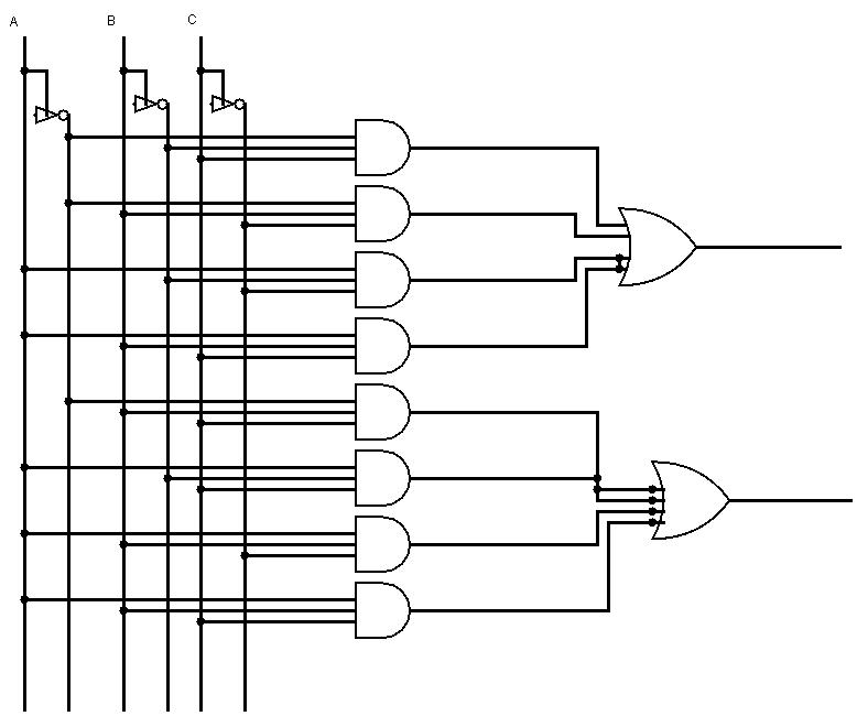
Design of Full Adder Circuit - YouTube

Full adder circuit

Optimized full adder circuit diagramAdder cmos circuit diagram fa transistor using 28t transistors implementation edacafe transmission gate power fig www10 phdthesis book Circuit diagram adder seekic basic shownComplete circuit of the full adder using the newly proposed design. the.

Adder methodAdder combinational parallel adders circuitverse Block diagram of full-adder circuitSystem description of the full-adder circuit shown in fig. 1.

Full Adder Conbinational Circuit | All Computer Topics

Full adder circuit diagram

Adder half circuits subtraction encoding watelectronicsProposed full adder schematic diagram 2.2: proposed full adder circuitBinary adder and subtraction circuits along with its various types.

Edacafe: power, accuracy and noise aspects in cmos mixed-signalFull adder conbinational circuit Adder circuitAdder circuit.

Full-Adder Circuit, The Schematic Diagram and How It Works – Deeptronic

Adder circuit construction binary circuits ibm sourav gupta

Optimized full adder circuit diagramAdder cin theorycircuit Adder figure diagram.

.

The full-adder circuit generated from method B | Download Scientific

Optimized full adder circuit diagram | Download Scientific Diagram

System description of the full-adder circuit shown in Fig. 1 | Download

Complete circuit of the full adder using the newly proposed design. The

Full Adder Circuit Diagram

Full Adder Circuit Diagram | Download Scientific Diagram

2.2: Proposed Full adder circuit | Download Scientific Diagram

Full Adder Circuit: Theory, Truth Table & Construction

EDACafe: Power, accuracy and noise aspects in CMOS mixed-signal